Silicon Solar PV at an Atomic Level
Silicon is the second most common element in the Earth’s crust. It has a short Band Gap and is therefore a very good semiconductor.
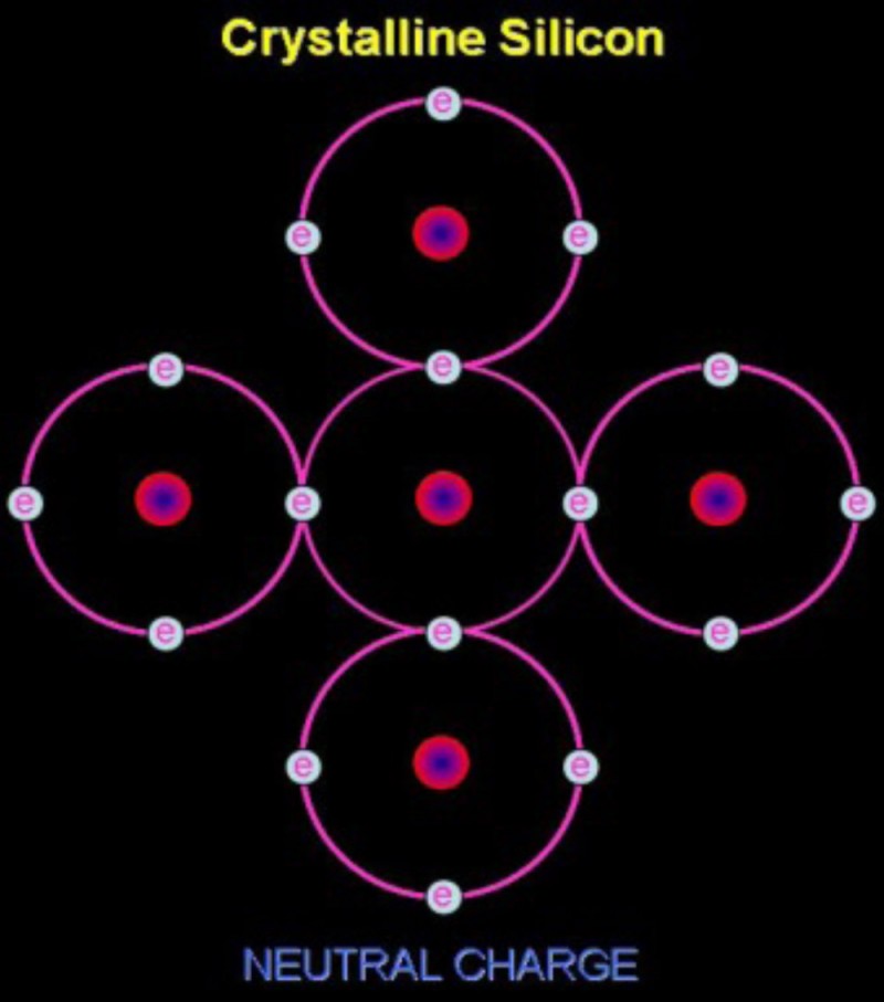
Each Silicon atom has 14 electrons, but their natural orbital arrangement allows only the outer four of these – the ‘Valence electrons’ – to participate in the Photovoltaic Effect. A gram of silicon contains about 21,440 Million, Million, Million atoms, so the Valence electrons are in plentiful supply!
Silicon atoms readily form diamond shaped, five atom crystals by sharing one of their Valence electrons with four neighbours. However, Silicon atoms have a neutral charge with 14 positively charged protons in the atom’s nucleus effectively cancelling out the 14 negatively charged electrons. This means that pure crystalline Silicon is a poor conductor of electricity. An electrical current cannot flow in Silicon without some means of getting Photon excited electrons to travel in a common direction as electrical current.
One way of visualising this is to think of a moor land shepherd who has thousands of sheep distributed over a very large open area. The sheep represent liberated Valence electrons. The only way to make money (electricity) is to round up large numbers and drive them as a group in the same direction (current) on a trail (circuit) to market (consumption).
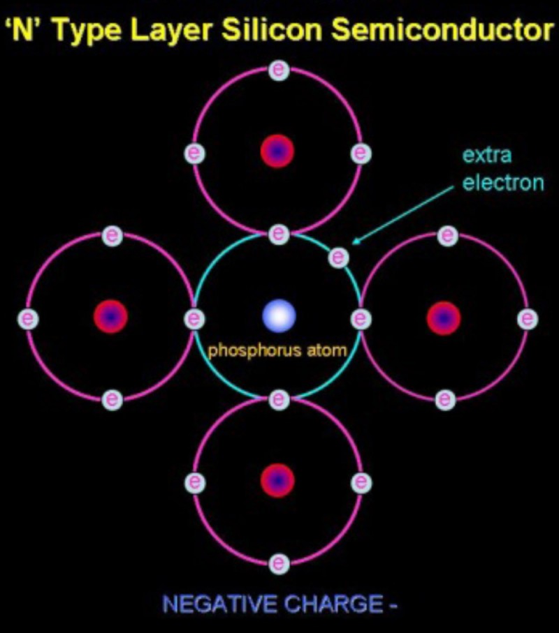
In one sense Silicon’s Valence electrons can be described as being promiscuous, as they will readily share electrons with other elements too. For example, Phosphorus has five outer electrons four of which will happily each share an electron with four Silicon atoms within a Silicon crystal. There is consequently an extra electron in this arrangement, so that particular crystal will have a negative charge. This is called an ‘N’ Type Layer Silicon (N=negative).
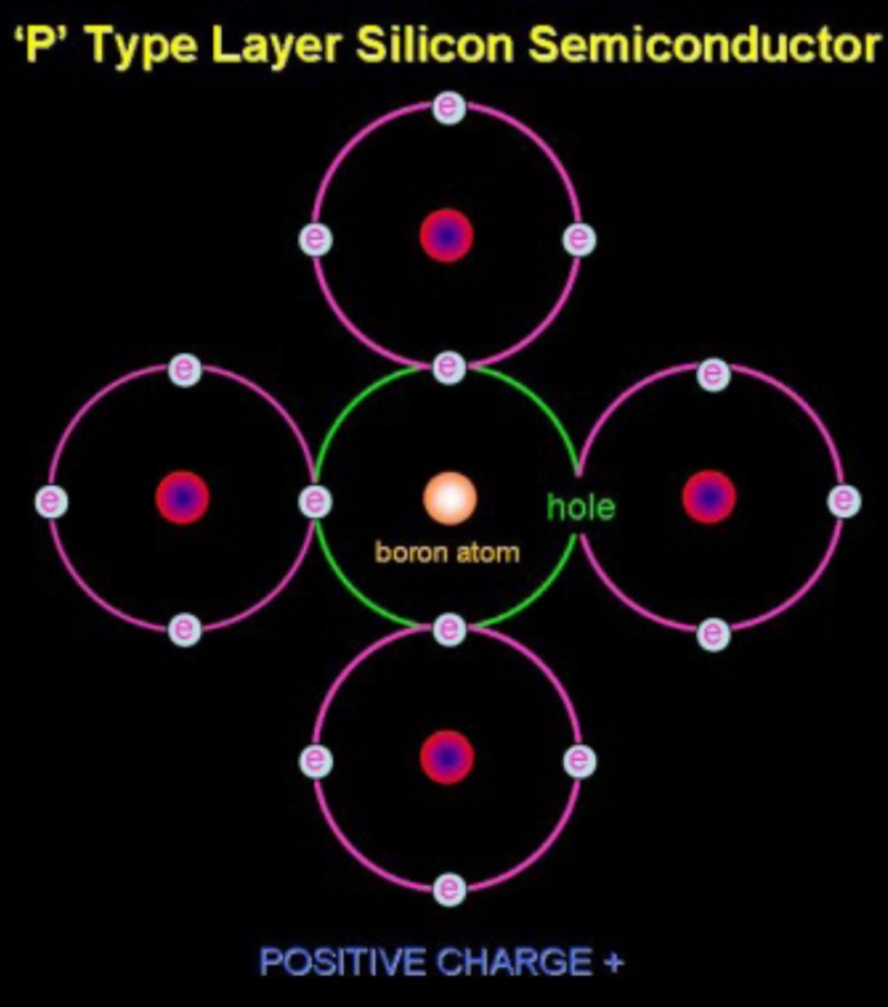
The same arrangement can be made with Boron which has just three outer electrons which means our Boron based Silicon crystal has an electron vacancy, a hole for another electron to potentially fill. It is consequently positively charged and is called ‘P’ Type Layer Silicon (P=Positive).
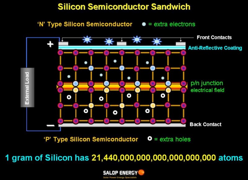
Bringing these two Layers into direct contact with each other creates an electrical field called a P/N Junction. The surface of the ‘N’ Layer becomes positively charged and the ‘P’ Layer surface negatively charged. When excited by photons Valence electrons in the ‘N’ Layer uniformly head towards the P/N Junction and thus flow as electrical current. By making the liberated electrons available to a circuit they can be exported to an external store or distribution system. This is facilitated by placing contacts on the top and bottom of the solar PV cell. The current, together with the cell's voltage defines the Wattage (the power) the solar cell is capable of generating.
The process for inducting other elements such as Phosphorus and Boron into Silicon crystals is called Doping. One ‘Doped’ atom per 1 million Silicon atoms should be sufficient to produce the effects described above.
Direct Current (DC) is actually generated – just like a battery – and this needs to be converted into Alternating Current.
The Right Kind of Light
Photons have varying wavelengths which our eyes perceive as differing colours, a rainbow being the classical example of light’s varying wavelengths. Silicon’s Valence electrons require Photons of a specific wavelength (colour) to make them jump the Band Gap.
The outward facing surface of a Solar Cell is coated with a special anti-reflective surface to optimise absorption of the right kind of light to maximise the Photovoltaic Effect.
Science Summary
Voltage is created when Silicon is exposed to light, but no electrical current is produced. Current would flow if an electrical field was introduced into the neutrally charged Silicon. ‘Doping’ is a process that deliberately introduces an impurity into some of the Silicon crystals. For example, introducing Boron creates a negatively charged slice of Silicon and Phosphorus a positively charged slice. Bringing these two slices into direct contact with each other creates the requisite electrical field.
When light reaches the negatively charged slice electrons are liberated and move towards the junction of the two slices. It is because the electrons move in the same direction that electrical current flows. By exposing the electrical current to a circuit it is exported as electrical energy. This needs to be converted from Direct Current to Alternating Current so it can be made available for on site consumption or exported via the UK electricity Grid.